
With the rapid growth in the number of new energy vehicles, DC fast-charging stations have become core infrastructure; consequently, the efficiency, power density, and reliability of their power modules directly determine the competitiveness of the ev charging station as a whole. Mainstream charging module power ratings in the industry have evolved from the early 15kW and 20kW levels to 30kW and 40kW, while 60kW single-module solutions are now seeing mass-market application in high-end fast-charging and ultra-fast-charging products. Taking the 60kW power module as an example, this article systematically outlines the design philosophy, key parameter selection, and practical implementation considerations for the “three-phase PFC + LLC resonant” two-stage architecture, serving as a reference for industry peers.
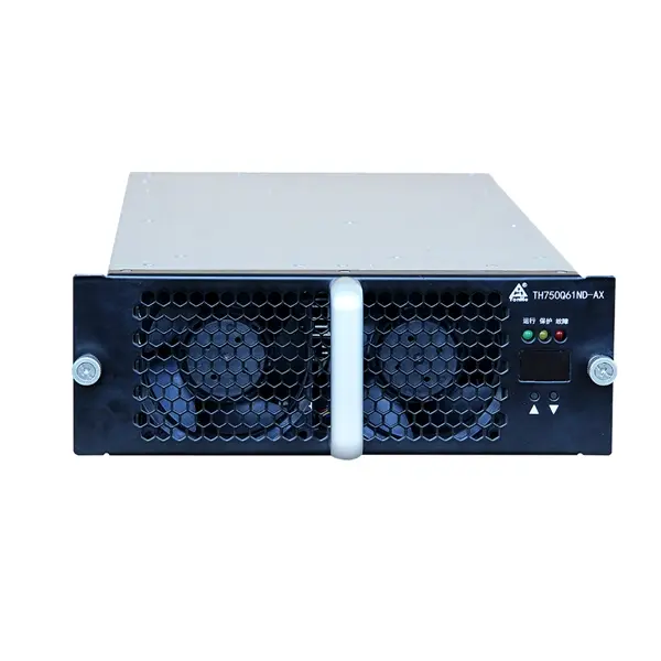
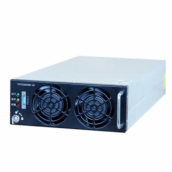
I. Overall Architecture and Design Specifications
The typical input and output specifications for the 60 kW module are as follows:
| Item | Parameter |
|---|---|
| Input | Three-phase four-wire 380VAC±15%, 47~63Hz |
| Output voltage range | 200~1000VDC (wide voltage coverage for passenger and commercial vehicles) |
| Output current | 0~150A (depends on the voltage platform) |
| Efficiency target | Peak ≥96%; full load range ≥95% |
| Power factor | ≥0.99 (above half load) |
| Power density | Target ≥1.2kW/L (forced air cooling) |
| Isolation withstand voltage | Input-to-output ≥3750VAC |
The overall topology consists of two stages: the front stage utilizes a three-phase interleaved parallel Boost PFC or a three-phase Vienna Rectifier to perform AC/DC conversion and power factor correction, outputting a stable DC bus (typically 770–800 V); the rear stage employs a full-bridge LLC resonant converter for DC/DC isolation and step-down, featuring a wide-gain design that covers an output range of 200–1000 V. A bus capacitor and current-sharing/communication interface are positioned between the two stages, while an integrated digital controller (utilizing a DSP/MCU dual-core or DSP+CPLD architecture) centrally manages the PFC voltage loop, the LLC dual-loop (voltage/current) control, and protection logic.
II. Front-end Three-phase PFC Design
1. Topology Selection
For the 60 kW power class, there are two common solutions for three-phase PFC:
- Three-level Vienna Rectifier
Unidirectional operation, low device voltage stress (half the DC bus voltage), and high efficiency; it is currently the mainstream choice for 60 kW charging modules. The drawback is that it operates only unidirectionally (does not support V2G inversion). - Three-phase Totem-pole / Interleaved Dual-Boost
Relatively simple structure; if SiC MOSFETs are used, full-bridge bidirectional operation is achievable. However, device voltage stress equals the DC bus voltage, and managing losses and EMI is more challenging.
If the module does not require V2G functionality, the Vienna Rectifier offers advantages in efficiency, cost, and thermal design; this article focuses on that topology.
2. Key Parameter Design
- Switching Frequency: Typically set between 32 kHz and 64 kHz to balance neutral-point potential stability against EMI filter size; with SiC devices, this can be increased to over 72 kHz to reduce inductor volume.
- Boost Inductor: Designed using a three-phase interleaved topology with independent inductors per phase; inductance values must balance current ripple (typically controlled at 20%–30% of rated current) against core losses, commonly utilizing high-frequency Sendust (Fe-Si-Al) or amorphous alloy cores.
- DC-Bus Capacitor: Must meet requirements for ripple current handling, hold-up time (typically ≥10 ms), and matching with the LLC stage resonant capacitor; a combination of film capacitors and metallized polypropylene capacitors in parallel is generally used.
- Neutral-Point Potential Balancing: A core control challenge for Vienna rectifiers; dynamic balancing is achieved through zero-sequence component injection or neutral-point current feedback to prevent uneven voltage stress across upper and lower switches, which could otherwise lead to component derating or failure.
3. Control Strategy
The front-end stage typically employs a dual-loop control structure consisting of an outer voltage loop and an inner current loop: the voltage loop stabilizes the DC-link voltage (770–800 V), while the current loop achieves sinusoidal current tracking with unity power factor, supplemented by a neutral-point balancing control loop. To enhance dynamic response, the prevailing trend is to upgrade from traditional PI control to a scheme combining voltage feed-forward with Quasi-Proportional Resonant (QPR) current control, thereby balancing steady-state accuracy with dynamic disturbance rejection capability.
III. Design of the Post-stage LLC Resonant Converter
1. Topology and Wide Gain Coverage
A 60kW LLC converter typically employs a full-bridge topology (half-bridge configurations are generally limited to modules under 20kW due to power density constraints). The core challenge lies in the fact that charging stations require a wide output voltage range (200–1000V), whereas the gain curve of a conventional LLC resonant converter peaks in efficiency near the resonant point; the further the operation deviates from resonance, the more both gain capability and efficiency degrade.
Three common engineering solutions exist:
- Wide-gain LLC with adjustable bus voltage: The front-end PFC bus voltage is adjusted within a specific range (e.g., 650–800V) based on output voltage requirements, thereby narrowing the gain range the LLC must actually cover;
- CLLC bidirectional topology: A secondary-side resonant network is added to the standard LLC structure, enabling both bidirectional energy flow (for V2G scenarios) and wide gain capability;
- Variable resonant parameters / Segmented design: Relays are used to switch resonant capacitors or transformer taps, splitting the wide operating range into high-voltage and low-voltage segments, with resonant parameters optimized separately for each.
For a strictly unidirectional 60kW fast-charging module, Solution 1 (coordinated PFC bus voltage regulation) combined with an optimized magnetizing inductance design currently offers the best cost-performance ratio.
2. Key Design Points for Resonant Parameters
- Quality Factor (Q): Typically designed within the 0.3–0.6 range; an excessively high Q narrows the gain range, while an excessively low Q results in an overly wide frequency modulation range under light loads and increased circulating current losses.
- Ratio of Magnetizing Inductance to Resonant Inductance (Ln = Lm/Lr): Directly determines the gain coverage capability; Ln is typically set between 3 and 6 for applications requiring a wide output range.
- Dead Time: Must ensure sufficient margin for ZVS (Zero Voltage Switching) while avoiding excessive dead time that would increase body diode conduction losses; generally set at 1%–3% of the switching frequency, with adaptive adjustments based on load current.
- Transformer Design: For the 60kW power level, planar transformers or matrix winding structures are recommended to minimize proximity effect losses; low-loss ferrite materials (such as PC95 or PC200) are commonly used for the cores, and particular attention must be paid to verifying leakage inductance consistency and temperature rise distribution across light-load and full-load conditions.
3. Synchronous Rectification
Replacing traditional diode rectification with SiC MOSFET-based synchronous rectification on the secondary side can significantly improve heavy-load efficiency by reducing conduction losses. This approach requires precise current zero-crossing detection and optimized gate-drive timing to prevent body-diode freewheeling losses and reverse current flow; it is typically implemented using a dedicated synchronous rectification (SR) controller in conjunction with a current transformer or DCR sensing.
IV. Recommendations for Key Component Selection
| Location | Recommended Components | Description |
|---|---|---|
| PFC switching tubes | 650V/750V SiC MOSFET | Reduces switching losses and supports higher switching frequency |
| LLC primary-side bridge arms | 900V~1200V SiC MOSFET | Provides margin for bus voltage fluctuation |
| LLC secondary-side synchronous rectification | Low on-resistance SiC / superjunction MOSFET | Matches current stress across a wide voltage range |
| Current sensing | Isolated Hall / isoAMP-type isolated amplifiers (e.g., AMC1200B/AMC1300 series) | Meets high-voltage isolation and fast protection response requirements |
| Main control | DSP (e.g., TMS320F28x series) + CPLD/FPGA auxiliary logic | Dual closed-loop control + fast hardware protection |
V. Thermal Design and Efficiency Optimization
For 60kW modules utilizing forced-air cooling, heat dissipation is the primary bottleneck in increasing power density. Common optimization strategies in engineering practice include:
- Loss Distribution Optimization: Using simulation to determine the specific loss contribution of components—such as PFC inductors, switching devices, LLC transformers, and rectifier diodes—allows for targeted optimization of thermal paths (e.g., employing independent air channels for transformers to prevent thermal coupling with switching devices);
- Current Sharing Design: When operating multiple modules in parallel, output current sharing accuracy must be ensured (typically requiring a tolerance within ±5%), usually achieved through droop control or master-slave communication;
- Efficiency Curve: The efficiency curve of a 60kW module typically peaks (at approximately 96%) within the 40%–70% load range; design efforts should prioritize efficiency at medium loads rather than focusing solely on the full-load point, as the module operates under partial-load conditions for extended periods in actual application.
VI. Common Engineering Issues and Debugging Points
- Bus Neutral-Point Voltage Imbalance: A common fault in Vienna rectifiers; requires checking the consistency between the zero-sequence injection algorithm and the three-phase current sampling.
- LLC Detuning/Audible Noise at Light Load: The switching frequency deviates significantly from the resonant point under light-load conditions; requires optimizing the burst mode or intermittent operation strategy.
- Synchronous Rectification Malfunction: Current zero-crossing detection is susceptible to noise interference across wide voltage ranges; requires enhanced drive signal filtering and adaptive dead-time control.
- EMI Exceeding Limits: Common-mode noise in three-level PFCs primarily stems from neutral-point potential fluctuations; requires optimizing Y-capacitor configuration and common-mode inductors, as well as adding active EMI filtering if necessary.
Conclusion
The PFC+LLC two-stage architecture for 60kW charging modules strikes an optimal balance among efficiency, power density, and cost, representing the industry’s mainstream technical approach. As the cost of SiC devices decreases and digital control algorithms mature, future charging modules will evolve toward higher switching frequencies, increased power densities (utilizing liquid cooling solutions), and bidirectional V2G capabilities. It is hoped that the design concepts presented here will serve as a useful reference for engineering practices in the field; further discussion and exchange of ideas are welcome.
Post time: Sep-03-2026


